1. The single-chip integrated circuit process uses a complete set of planar process technologies such as grinding, polishing, oxidation, diffusion, photolithography, epitaxial growth, and evaporation to simultaneously manufacture transistors, diodes, resistors, capacitors, and other components on a small silicon single crystal wafer, and uses certain isolation techniques to isolate each component from each other in terms of electrical performance. Tad, layer aluminium evaporatus est super superficiem wafer silicon is et in pattern interconnectus utilizant technologiam photolithographiae, permittant componentes connectare in circuitu completum, ut necesse est, et semiconductorem circuitum singulam chipom integratum.
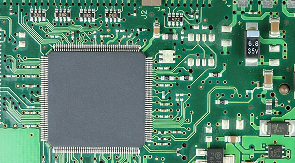
circuit singula chipa integrata
With the development of single-chip integrated circuits from small to medium scale to large-scale and ultra large scale integrated circuits, planar process technology has also been developed. Exemplo, diffusion doping replacetur ion implantatio doping process; Lithographia UV conventional in multum technologiarum microfabricationis, quasi plateam exposurae electronis, etching plasma, reactive ion milling, etc. Epitaxial growth also adopts ultra-high vacuum molecular beam epitaxy technology; Using chemical vapor deposition technology to manufacture polycrystalline silicon, silicon dioxide, and surface passivation films; In addition to using aluminum or gold, the interconnect thin lines also adopt processes such as chemical vapor deposition heavily doped polycrystalline silicon thin films and precious metal silicide thin films, as well as multi layer interconnect structures.
circuit singula chipa integrata circuit integrata est, qui independentem functiones circuit unius sine necessitate componentibus externis implementat. To achieve single-chip integration, it is necessary to address the integration of resistors, capacitors and power devices that are difficult to miniature, as well as the issue of isolating each component from the other in terms of circuit performance.
2. The transistor, diode, resistor, capacitor, inductor and other components of the entire circuit, as well as their interconnections, are all made of metal, semiconductor, metal oxide, various metal mixed phases, alloys or insulating dielectric films with a thickness of less than 1 micron, and overlapped by vacuum evaporation process, sputtering process and electroplating process. Circuit integratus ex hoc processo cinematographica circuitus integratus appellatur. Processus principis:
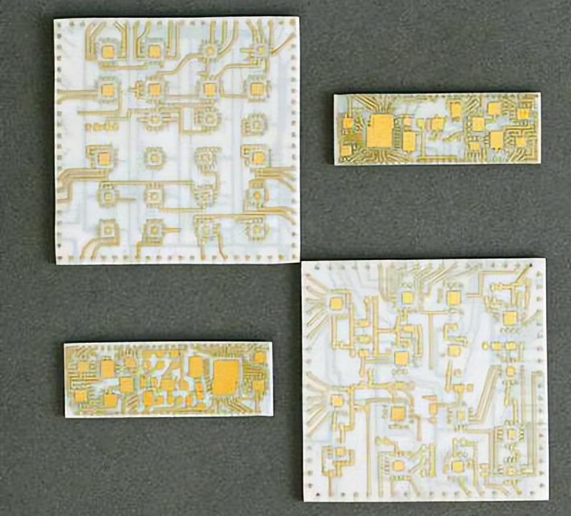 Thin Film Integrated Circuit
* 9312; According to the circuit diagram, first divide it into several functional component diagrams, then use the planar layout method to convert them into planar circuit layout diagrams on the substrate, and then use the photographic plate making method to produce thick film network templates for screen printing
●9313;The main processes for manufacturing thick film networks on substrates are printing, sintering, and resistance tuning. Metodo imprentae usus est imprenta schermi.
●9314;During the sintering process, the organic binder completely decomposes and evaporates, and the solid powder melts, decomposes, and combines to form a dense and strong thick film. Carmen pellicularum qualitate et actione coniunctae sunt sinteri procedenti et atmosferi ambiente. Calefactio tempore lentem esse ut perfectam eliminationem organicae antequam vitrum fluit. Tempus sinterium et temperatura maxima dependunt super structuram vulnerae et membranei utilizatam. In order to prevent cracking of the thick film, the cooling rate should also be controlled. fornacia sinterna saepe utilita est clanca tunelae.
●9315;To achieve optimal performance of thick film networks, resistors need to be adjusted after firing. Common resistance adjustment methods include sandblasting, laser, and voltage pulse adjustment.
3. Thick film integrated circuit technology uses screen printing to deposit resistance, dielectric, and conductor coatings on aluminum oxide, beryllium oxide ceramics, or silicon carbide substrates. The deposition process involves using a fine wire mesh to create patterns of various films. Haec parabola facit per modos photographicas, et latex utilitur ut bloqueretur holas mesh in omnibus regionibus ubi nulla vestimenta deposita est. After cleaning, the alumina substrate is printed with conductive coating to form internal connection lines, resistor terminal soldering areas, chip adhesion areas, capacitor bottom electrodes, and conductor films. Post siccationem, partes in temperatura inter 750 et 950 °C coquuntur ut formarent, evaporant adhesivas, sinterent materiales conductores, et tunc imprentationes et firandos faciant resistores, capacitores, saltatores, insulatores et signos colores. Active devices are fabricated using processes such as low eutectic welding, reflow soldering, low melting point bump inversion soldering, or beam type lead, and then mounted on a burned substrate. The leads are then soldered to form thick film circuits.
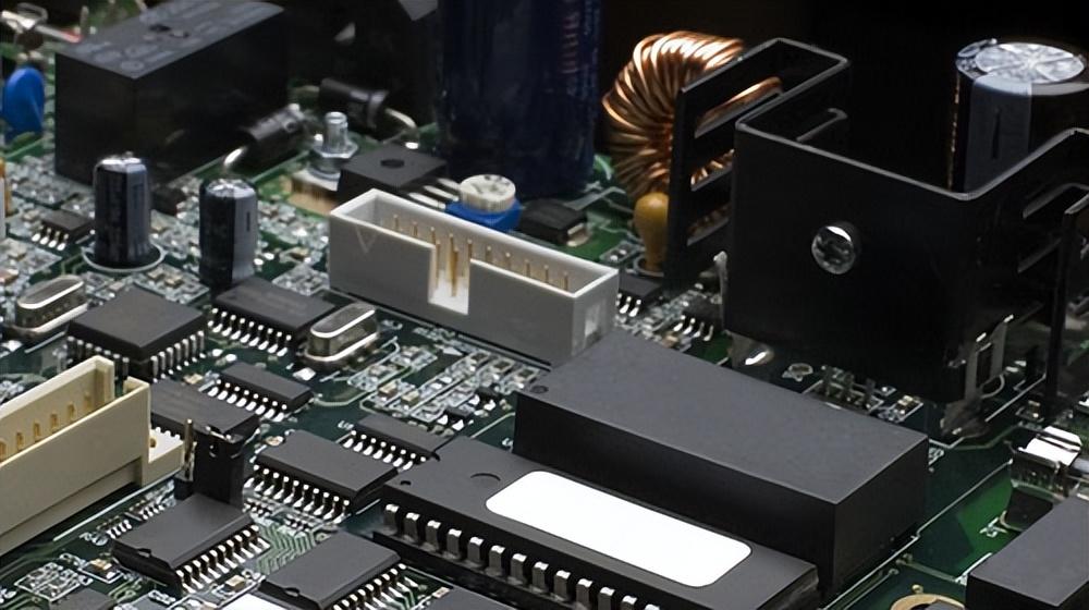 thick film integrated circuit
Densita pelliculae circulatorum densorum cinematographicae generale 7-40 micronus est. The process of preparing multi layer wiring using thick film technology is relatively convenient, and the compatibility of multilayer technology is good, which can greatly improve the assembly density of secondary integration. In addition, plasma spraying, flame spraying, printing and pasting processes are all new thick film process technologies. Similar to thin film integrated circuits, thick film integrated circuits also use hybrid processes because thick film transistors are not yet practical.
4. Characteristica procedurae: circulos singulos chips et cinematographicos thinos et circulos densos integros singulos habent proprias caracterias et inter se complemente potent. Quantitas circulatorum generalium et circulatorum standardisum magnum est, et circulatus singulae chipi integrae utilizatur. For low demand or non-standard circuits, a hybrid process is generally used, which involves using standardized single-chip integrated circuits and hybrid integrated circuits with active and passive components. Silah film ve thin film integrated circuits intersect each other in certain applications. The process equipment used in thick film technology is relatively simple, the circuit design is flexible, the production cycle is short, and the heat dissipation is good. Therefore, it is widely used in circuits with high voltage, high power, and less stringent tolerance requirements for passive components. In addition, due to the ease of achieving multi-layer wiring in the manufacturing process of thick film circuits, large-scale integrated circuit chips can be assembled into ultra large scale integrated circuits in more complex applications beyond the capabilities of single-chip integrated circuits. Single or multifunctional single-chip integrated circuit chips can also be assembled into multifunctional components or even small machines.
5. Utrum et precautiones: (1) Circulae integrae non sunt permittit transire limita eorum in uso. Quando electricae constituit voltage non plus quam 10% de valore nomine, parametros electricae conformentur ad nomina valora. When the power supply used in the circuit is turned and off, there must be no instantaneous voltage generated, otherwise it will cause the circuit to break down.
(2) Temperatura operationis circulatorum integrorum est generale inter -30~85 °C, et illos cum possibile longe ab fontes calefactis installentur.
(3) When manually soldering integrated circuits, soldering irons with a power greater than 45W should not be used, and the continuous soldering time should not exceed 10 seconds.
(4) For MOS integrated circuits, it is necessary to prevent gate electrostatic induction breakdown.
Superior est introduccio tecnologiae circuit integrae. In hoc tempore circuits unic chip integratae non solum ad altum integrationem, sed etiam ad altum potentiam, linearum, circuitum altum frequencatis et circuitum analogorum developerunt. However, in terms of microwave integrated circuits and high-power integrated circuits, thin film and thick film hybrid integrated circuits still have advantages. In specific selection, various types of single-chip integrated circuits are often combined with thick film and thin film integration processes, especially precision resistor network and resistor capacitor network substrates are attached to substrates assembled from thick film resistors and conduction bands to form a complex and complete circuit. When necessary, individual ultra small components can even be connected to form parts or the entire machine.


 English
 Spanish
 Arabic
 French
 Portuguese
 Belarusian
 Japanese
 Russian
 Malay
Malay Icelandic
 Bulgarian
 Azerbaijani
 Estonian
 Irish
Irish Polish
 Persian
 Boolean
 Danish
 German
 Filipino
 Finnish
 Korean
 Dutch
Dutch Galician
 Catalan
 Czech
Czech Croatian
 Latvian
 Romanian
 Maltese
 Macedonian
 Norwegian
 Swedish
 Serbian
 Slovak
 Slovenian
 Swahili
 Thai
Thai Turkish
 Welsh
Welsh Urdu
Urdu Ukrainian
 Greek
Greek Hungarian
 Italian
 Yiddish
 Indonesian
 Vietnamese
 Haitian Creole
 Spanish Basque


