1. The single-chip integrated circuit process utilizes a complete set of planar process technologies such as grinding, polishing, oxidation, diffusion, photolithography, epitaxial growth, and evaporation to simultaneously manufacture transistors, diodes, resistors, capacitors, and other components on a small silicon single crystal wafer, and uses certain isolation techniques to isolate each component from each other in terms of electrical performance. Then, an aluminum layer is evaporated on the surface of the silicon wafer and etched into an interconnect pattern using photolithography technology, allowing the components to interconnect into a complete circuit as needed, and producing a semiconductor single-chip integrated circuit.
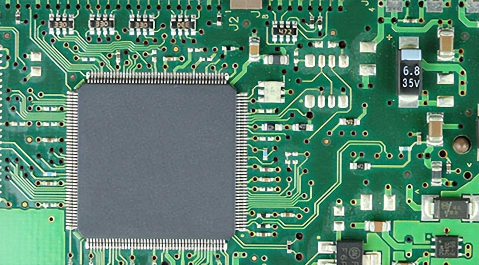
Single-chip integrated circuit
With the development of single-chip integrated circuits from small to medium scale to large-scale and ultra large scale integrated circuits, planar process technology has also been developed. For example, diffusion doping is replaced by ion implantation doping process; UV conventional lithography has developed into a complete set of microfabrication technologies, such as electron beam exposure plate making, plasma etching, reactive ion milling, etc; Epitaxial growth also adopts ultra-high vacuum molecular beam epitaxy technology; Using chemical vapor deposition technology to manufacture polycrystalline silicon, silicon dioxide, and surface passivation films; In addition to using aluminum or gold, the interconnect thin lines also adopt processes such as chemical vapor deposition heavily doped polycrystalline silicon thin films and precious metal silicide thin films, as well as multi-layer interconnect structures.
A single-chip integrated circuit is an integrated circuit that independently implements unit circuit functions without the need for external components. To achieve single-chip integration, it is necessary to address the integration of resistors, capacitors, and power devices that are difficult to miniaturize, as well as the issue of isolating each component from each other in terms of circuit performance.
2. The transistor, diode, resistor, capacitor, inductor and other components of the entire circuit, as well as their interconnections, are all made of metal, semiconductor, metal oxide, various metal mixed phases, alloys or insulating dielectric films with a thickness of less than 1 micron, and overlapped by vacuum evaporation process, sputtering process and electroplating process. The integrated circuit made by this process is called a thin film integrated circuit. Main process:
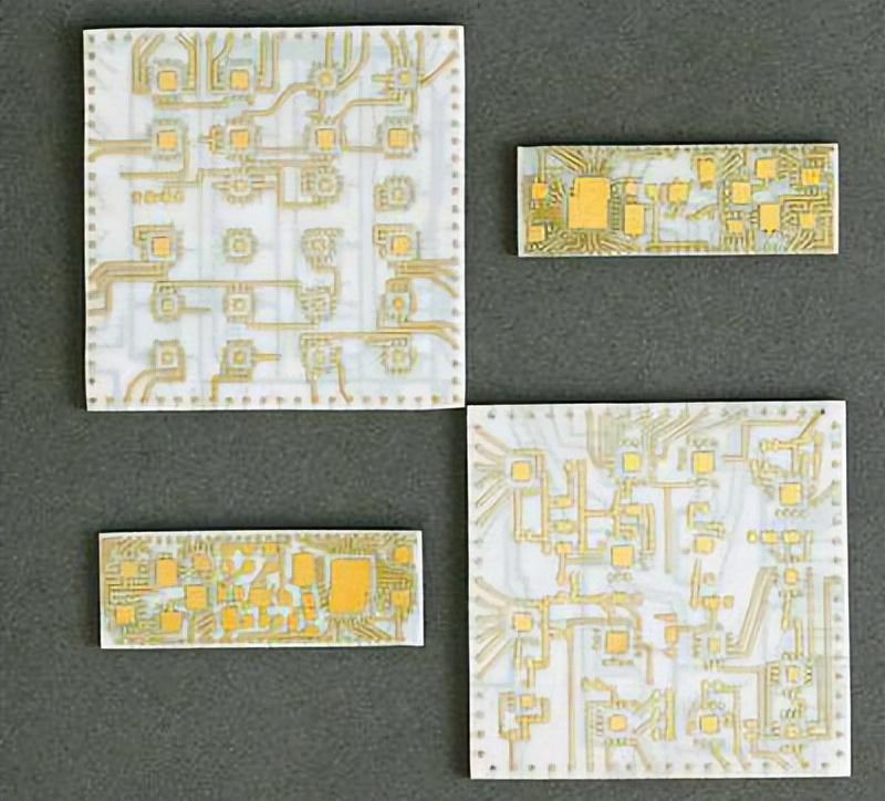 Thin Film Integrated Circuit
① According to the circuit diagram, first divide it into several functional component diagrams, then use the planar layout method to convert them into planar circuit layout diagrams on the substrate, and then use the photographic plate making method to produce thick film network templates for screen printing
② The main processes for manufacturing thick film networks on substrates are printing, sintering, and resistance tuning. The commonly used printing method is screen printing.
③ During the sintering process, the organic binder completely decomposes and evaporates, and the solid powder melts, decomposes, and combines to form a dense and strong thick film. The quality and performance of thick films are closely related to the sintering process and environmental atmosphere. The heating rate should be slow to ensure the complete elimination of organic matter before the glass flows; The sintering time and peak temperature depend on the slurry and membrane structure used. To prevent cracking of the thick film, the cooling rate should also be controlled. The commonly used sintering furnace is the tunnel kiln.
④ To achieve optimal performance of thick film networks, resistors need to be adjusted after firing. Common resistance adjustment methods include sandblasting, laser, and voltage pulse adjustment.
3. Thick film integrated circuit technology uses screen printing to deposit resistance, dielectric, and conductor coatings on aluminum oxide, beryllium oxide ceramics, or silicon carbide substrates. The deposition process involves using a fine wire mesh to create patterns of various films. This pattern is made using photographic methods, and latex is used to block the mesh holes in any areas where no coating is deposited. After cleaning, the alumina substrate is printed with conductive coating to form internal connection lines, resistor terminal soldering areas, chip adhesion areas, capacitor bottom electrodes, and conductor films. After drying, the parts are baked at a temperature between 750 and 950 ℃ to form, evaporate the adhesive, sinter the conductor material, and then use printing and firing processes to produce resistors, capacitors, jumpers, insulators, and color seals. Active devices are fabricated using processes such as low eutectic welding, reflow soldering, low melting point bump inversion soldering, or beam type lead, and then mounted on a burned substrate. The leads are then soldered to form thick film circuits.
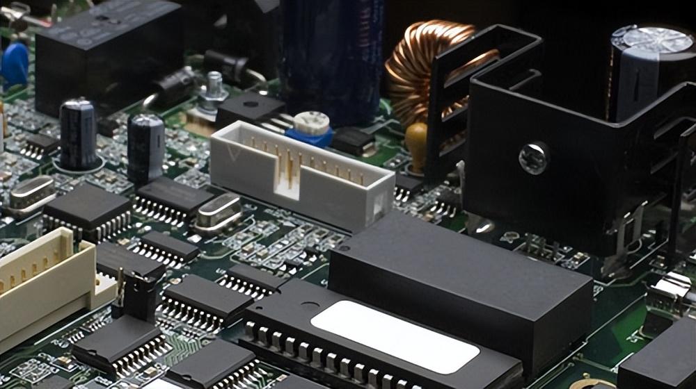 thick film integrated circuit
The film thickness of thick film circuits is generally 7-40 microns. The process of preparing multi-layer wiring using thick film technology is relatively convenient, and the compatibility of multi-layer technology is good, which can greatly improve the assembly density of secondary integration. In addition, plasma spraying, flame spraying, printing and pasting processes are all new thick film process technologies. Similar to thin film integrated circuits, thick film integrated circuits also use hybrid processes because thick film transistors are not yet practical.
4. Process characteristics: Single chip integrated circuits and thin film and thick film integrated circuits each have their own characteristics and can complement each other. The quantity of general circuits and standard circuits is large, and single-chip integrated circuits can be used. For low demand or non-standard circuits, a hybrid process is generally used, which involves using standardized single-chip integrated circuits and hybrid integrated circuits with active and passive components. Thick film and thin film integrated circuits intersect with each other in certain applications. The process equipment used in thick film technology is relatively simple, the circuit design is flexible, the production cycle is short, and the heat dissipation is good. Therefore, it is widely used in circuits with high voltage, high power, and less stringent tolerance requirements for passive components. In addition, due to the ease of achieving multi-layer wiring in the manufacturing process of thick film circuits, large-scale integrated circuit chips can be assembled into ultra large scale integrated circuits in more complex applications beyond the capabilities of single-chip integrated circuits. Single or multifunctional single-chip integrated circuit chips can also be assembled into multifunctional components or even small machines.
5. Usage and precautions: (1) Integrated circuits are not allowed to exceed their limit values during use. When the power supply voltage changes by no more than 10% of the rated value, the electrical parameters should comply with the specified values. When the power supply used in the circuit is turned on and off, there must be no instantaneous voltage generated, otherwise it will cause the circuit to break down.
(2) The operating temperature of integrated circuits is generally between -30~85 ℃, and they should be installed as far away from heat sources as possible.
(3) When manually soldering integrated circuits, soldering irons with a power greater than 45W should not be used, and the continuous soldering time should not exceed 10 seconds.
(4) For MOS integrated circuits, it is necessary to prevent gate electrostatic induction breakdown.
The above is an introduction to integrated circuit technology. At present, single-chip integrated circuits are not only developing towards higher integration, but also towards high-power, linear, high-frequency circuits and analog circuits. However, in terms of microwave integrated circuits and high-power integrated circuits, thin film and thick film hybrid integrated circuits still have advantages. In specific selection, various types of single-chip integrated circuits are often combined with thick film and thin film integration processes, especially precision resistor network and resistor capacitor network substrates are attached to substrates assembled from thick film resistors and conduction bands to form a complex and complete circuit. When necessary, individual ultra small components can even be connected to form parts or the entire machine.


 Spanish
 Arabic
 Spanish Basque
 Portuguese
 Belarusian
 Japanese
 Russian
 Icelandic
 Bulgarian
 Azerbaijani
 Estonian
 Irish
Irish Polish
 Persian
 Boolean
 Danish
 German
 French
 Filipino
 Finnish
 Korean
 Dutch
Dutch Galician
 Catalan
 Czech
Czech Croatian
 Latin
Latin Latvian
 Romanian
 Maltese
 Malay
Malay Macedonian
 Norwegian
 Swedish
 Serbian
 Slovak
 Slovenian
 Swahili
 Thai
Thai Turkish
 Welsh
Welsh Urdu
Urdu Ukrainian
 Greek
Greek Hungarian
 Italian
 Yiddish
 Indonesian
 Vietnamese
 简体中文
简体中文 Haitian Creole

